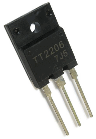
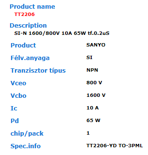
Part Number : TT2206
NPN Triple Diffused Planar Silicon Transistor.
Function is High Voltage Color Display Horizontal Deflection Output.
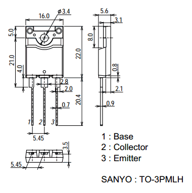
Package : TO-3P MLH Type
Features
1. High speed.
2. High breakdown voltage (Vcbo=1600V, Vceo=800V, Ic=10A, Pc=65W ).
3. High reliability (Adoption of HVP process).
4. Adoption of MBIT process.
5. On-chip damper diode.
The equivalent circuit is 2SС5793, TT2202, JL6920, 2SC5446, FJAF6810, FJAF6820.
( TT2202 is Vcbo = 1500V, Vceo=800V )
Транзистор биполярный (аналог 2SC5793)
Reference PDF :
#1 : Sanyo TT2202 datasheet pdf
#2 : Sanyo 2SC5793 datasheet pdf
#3 : Toshiba 2SC5446 datasheet pdf
#4 : Fairchild FJAF6810 datasheet pdf


