TLC555 PDF – Low Power Timer – TI

Part Number : TLC555

Function : Low Power Timer / LinCOMS TIMER – TLC555

Manufacturer : Texas Instruments

Pinout :
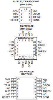
TLC555 datasheet

Description

Description
The TLC555 is a monolithic timing circuit fabricated using the TI LinCMOSprocess. The timer is fully compatible with CMOS, TTL, and MOS logic and operates at frequencies up to 2 MHz.

Because of its high input impedance, this device uses smaller timing capacitors than those used by the NE555.

As a result, more accurate time delays and oscillations are possible. Power consumption is low across the full range of power supply voltage.

Features
. Very Low Power Consumption
− 1 mW Typ at VDD= 5 V

. Capable of Operation in Astable Mode
. CMOS Output Capable of Swinging Rail to Rail
. High Output-Current Capability
− Sink 100 mA Typ
− Source 10 mA Typ

. Output Fully Compatible With CMOS, TTL, and MOS
. Low Supply Current Reduces Spikes During Output Transitions
. Single-Supply Operation From 2 V to 15 V
. Functionally Interchangeable With the NE555; Has Same Pinout
. ESD Protection Exceeds 2000 V Per MIL-STD-883C, Method 3015.2
.Available in Q-Temp Automotive

High Reliability Automotive Applications
Configuration Control/Print Support
Qualification to Automotive Standards

TLC555 Datasheet PDF Download

TLC555 pdf

Other datasheets in the file : 555, 5962-89503012A, 8950301PA, P555

Datasheet PDF

LM124AJ Schematic

Part Number : LM124AJ

Function : QUAD GENERAL PURPOSE BIPOLAR OPERATIONAL AMPLIFIER

Manufacturer : Texas Instruments

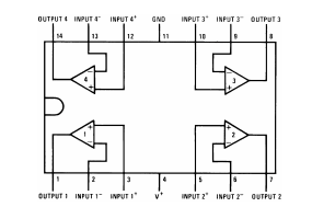
Pinout :

LM124AJ datasheet

Description

Description

These devices consist of four independent high-gain frequency-compensated operational amplifiers that are designed specifically to operate from a single supply over a wide range of voltages. Operation from split supplies also is possible if the difference between the two supplies is 3 V to 32 V (3 V to 26 V for the LM2902 device), and VCC is at least 1.5 V more positive than the input common-mode voltage. The low supply-current drain is independent of the magnitude of the supply voltage.

Applications include transducer amplifiers, dc amplification blocks, and all the conventional operational-amplifier circuits that now can be more easily implemented in single-supply-voltage systems. For example, the LM124 device can be operated directly from the standard 5-V supply that is used in digital systems and provides the required interface electronics, without requiring additional ±15-V supplies.

Features

2-kV ESD Protection for: LM224K, LM224KA
LM324K, LM324KA
LM2902K, LM2902KV, LM2902KAV

Wide Supply Ranges Single Supply: 3 V to 32 V (26 V for LM2902)
Dual Supplies: ±1.5 V to ±16 V
(±13 V for LM2902)

Low Supply-Current Drain Independent of
Supply Voltage: 0.8 mA Typ
Common-Mode Input Voltage Range Includes Ground,
Allowing Direct Sensing Near Ground
Low Input Bias and Offset Parameters Input Offset Voltage: 3 mV Typ
A Versions: 2 mV Typ
Input Offset Current: 2 nA Typ
Input Bias Curren: 20 nA Typ
A Versions: 15 nA Typ

Differential Input Voltage Range Equal
to Maximum-Rated Supply Voltage: 32 V
(26 V for LM2902)
Open-Loop Differential Voltage Amplification:
100 V/mV Typ
Internal Frequency Compensation
On Products Compliant to MIL-PRF-38535, All
Parameters Are Tested Unless Otherwise Noted.
On All Other Products, Production Processing
Does Not Necessarily Include Testing of All
Parameters.

Datasheet PDF Download

LM124AJ pdf

Other datasheets in the file :
LM124,LM124AJ-PB,LM124J-PB,LM224,LM224J
Datasheet PDF